How iFixit Uses a Digital Microscope to Reveal What’s Inside Your Phone
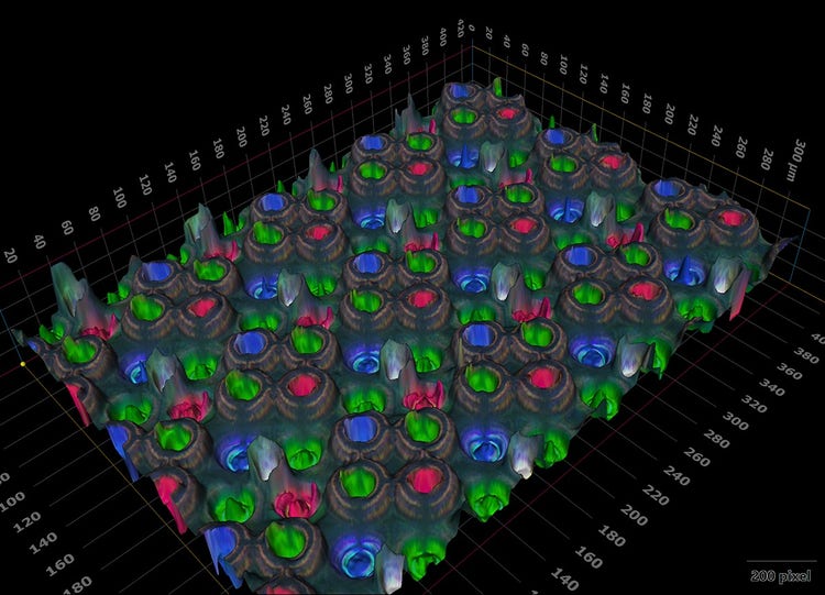
3D microscope image of the Samsung Galaxy S26 Ultra display created using Z-stacking on the DSX2000 digital microscope.

What a Digital Microscope Adds to a Phone Teardown
You take it apart, put it under a microscope, and look at the parts nobody was meant to see.
Every year, manufacturers tell us what is inside their newest devices. Marketing graphics show a privacy layer here, a vapor chamber there, and a clever adhesive somewhere else. The diagrams are clean and convincing. They are also decided in advance by the people who built the product. iFixit exists to check. The team has been taking consumer electronics apart in public for years, scoring each device on how repairable it is and publishing the evidence for anyone to see.
Manufacturers pay attention to those scores, which is exactly why the evidence must hold up. And much of what decides whether a phone can be repaired happens at a scale no phone camera can reach: an adhesive bead, a coating, the way a display stack is layered.
To capture that level of detail, iFixit uses the DSX2000 digital microscope. We spoke with Arthur Shi, senior technical writer at iFixit, about how the microscope fits into a teardown, what it has revealed inside recent flagship phones, and the moment a Samsung marketing graphic did not match what the team found underneath.
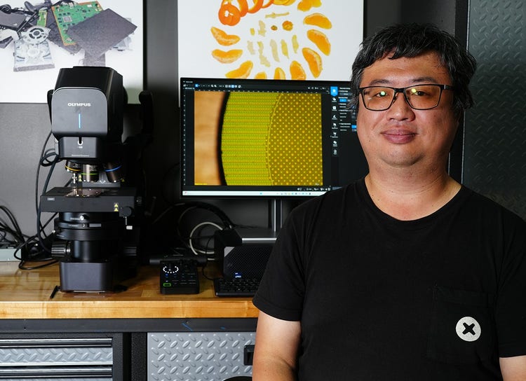
Arthur Shi at the DSX2000 digital microscope in iFixit's teardown lab.
Meet Arthur Shi, Senior Technical Writer at iFixit
Arthur: I help take apart various devices and gadgets to have a quick educational look at how they're designed and how repairable they are, and to analyze and help demystify the tech that's in these devices. My background is a master's in electrical engineering, and photography is a hobby of mine, so I tend to be the one behind the microscope, working out what we're actually looking at and turning it into images people can understand.
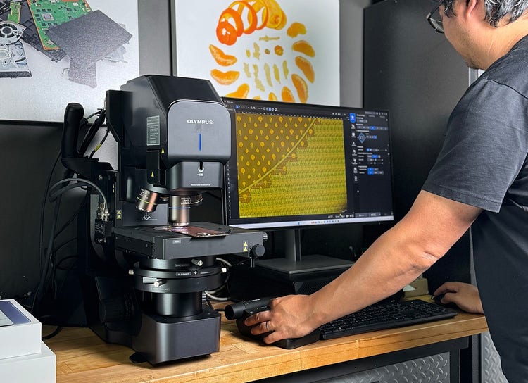
Arthur Shi at work on the DSX2000 digital microscope during a phone teardown.
How does digital microscopy fit into the phone teardown workflow? When does the microscope come in?
Arthur: It's a discovery and exploration phase, really. As we're taking apart the device, we're bringing it into the microscope and taking a close look and figuring out the analysis on the way. It's not something we save for the end. The microscope is on the bench the whole time, and the moment something looks unusual, it goes under the objective so we can see what's going on.
Before you switched to the DSX2000 digital microscope, what was missing from your teardown imaging process?
Arthur: We simply couldn't get the images. We either had to bypass that aspect of the analysis, or we used a very basic microscope, which didn't show as much. So, we'd hedge in the writing and illustrate with drawings instead. It worked, but it wasn't the same as showing the real thing. Microscope images always get a lot more attention. People see them on social media, and they're always excited to see the actual thing.
You recently completed a Samsung Galaxy S26 Ultra teardown. Could you describe the imaging process used to visualize the privacy display panel?
Arthur: The privacy screen was the thing we wanted to showcase, so the display panel went under first. We imaged it from the front and then from the back. Samsung had its marketing graphics showing how it looks, but we weren't sure how they actually implemented it through the structure. Once we imaged both sides, we could see where the privacy layer really sat in the stack, and it was higher than we'd assumed. The privacy pixels shared a stack with the standard pixels, and the physical cones that restrict the viewing angle were doing the real work.
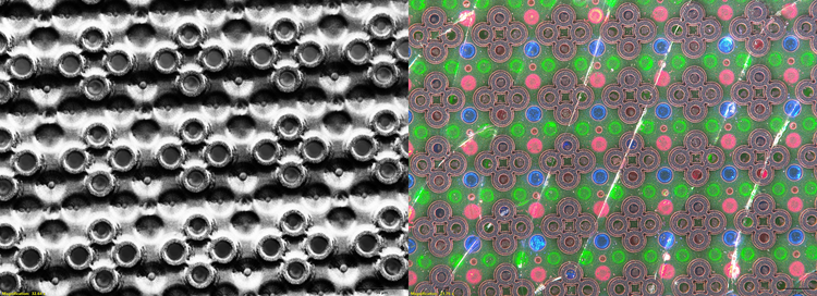
The S26 Ultra display panel from the front. Left: In shaded relief mode, the rings around each privacy pixel that prevent light from escaping sideways are visible. Right: RGB subpixels shown in MIX mode, also known as MIX illumination.
When you captured images inside the S26 Ultra display, you noticed unusual color in the OLED panel. Could you explain what you found?
Arthur: Yes. Under reflected light, the panel showed color, which was very strange for an OLED because it's self-emissive and doesn't really need color filters. It looked like they had color filters still on the pixels. I think they did it to increase contrast or reduce reflections. We tried polarized light and found no polarizing effect, but we did see color banding coming off the coatings. We were careful about how we presented that in the teardown, but we only had something to investigate because we could see it in the first place.
The privacy layer resolved as a 3D image, created using Z-stacking. It sits higher in the panel than expected, with each peak representing a single subpixel.
In the iPhone 17 Pro teardown, what causes the camera plateau to scratch?
Arthur: The anodized aluminum around the camera plateau was chipping when it met keys and coins. We wanted to show what was physically happening at that edge, so we imaged the aluminum lip and caught the coating shearing away from the sharp corner. At that magnification, you can't get enough of the thing in focus on its own, so we used the stacking capability to get a nice depth of field. That's what made the images usable.
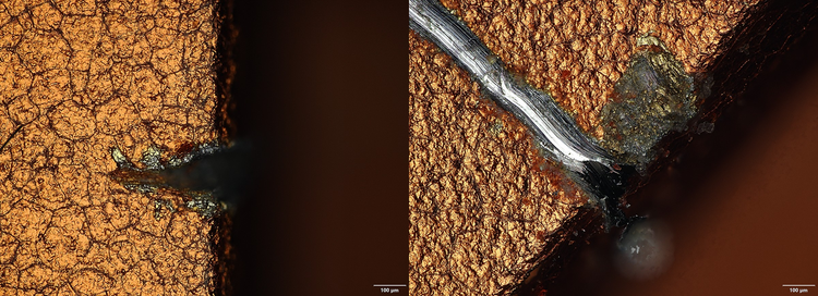
Under a Mohs level-4 pick, roughly the hardness of a coin, the anodized coating chips away at the sharp edge of the camera plateau to reveal bare aluminum. Imaged at 20X in MIX mode.
Inside the iPhone 17 Pro Vapor Chamber
The same teardown put the iPhone 17 Pro’s cooling hardware under the objective. Imaging revealed the internal copper wick structure that moves heat away from the processor.
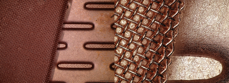
Left: Inside the iPhone 17 Pro's vapor chamber, a woven copper lattice wicks and condenses the working fluid that carries heat away from the chip. Right: The same chamber at higher magnification. Both images were captured in brightfield.

Recorded live in 4K on the DSX2000 digital microscope, the S26 Ultra display panel is shown powering on and off, revealing the privacy structure at work in real time.
What DSX2000 features do you use daily, such as optics, imaging modes, or free-angle observation?
Arthur: The physical optics are great. I have a set of prime lenses that I can easily swap in for whatever purpose I want. The lighting does a lot of the work too. All the various lighting functions are really useful for drawing out details, because they all give different effects. I use shaded relief for a quick read on 3D structure, and most of my published images end up in MIX mode. The free-angle observation matters more than you'd think, because phone frames don't sit flat. Being able to tilt the optics instead of moving the sample is how we got into the iPhone Air chassis to show the machining inside.
What does 4K video add to a teardown?
Arthur: More than I expected. We record live 4K clips of the sample under the scope and drop them straight into the teardown videos. On the S26 Ultra, we powered the display panel on and off while it sat on the stage and filmed what the privacy structure does in real time. It creates a very dynamic look. It shows live what happens and what that looks like. On the older microscope, clips were capped at 10 seconds and uncompressed, so this is a real step up.
FineWoven vs. TechWoven: What did the microscope reveal about Apple’s cases?
Arthur: One of my favorites had nothing to do with the electronics. Apple's FineWoven cases were widely disliked because they stained, and the replacement, TechWoven, didn't have the problem. We put both under the microscope and could see that they changed the weave density completely and added a new coating. The FineWoven case wasn't sealed at all, so any liquid would absorb into the fibers. With the TechWoven cases, they sealed it, with a liquid-resistant layer on top. Two products, one obvious difference in everyday use, and you could point a camera right at the reason.
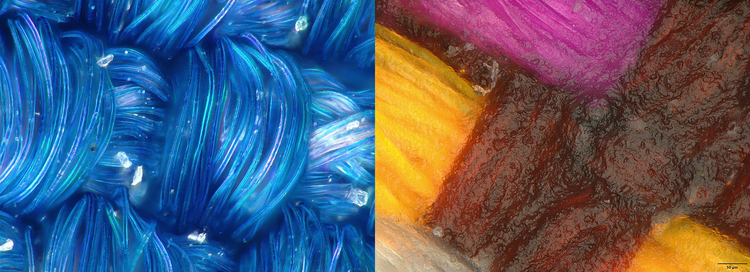
Left: FineWoven is an open and unsealed weave that lets liquids soak into the fibers. Right: TechWoven is a denser weave with a liquid-resistant coating on top. Both images were captured in MIX mode.
What was it like getting started with the DSX2000 digital microscope? How hard was it to learn?
Arthur: It's pretty intuitive, and it's pretty easy to get amazing-looking photos. There was an initial learning curve, not too bad. We'd used the previous generation, so a lot was familiar, and setup was handled remotely in about half an hour. Once everything is set up, it's amazingly easy to start using. We normally have it constantly on, and it just works.
What does digital microscope imaging let iFixit prove?
Arthur: Our main goal is to educate people, so creating striking imagery, anything that helps, is really helpful. The images carry the story. They let us settle arguments about how something is built, and they get people genuinely interested in what's inside their devices. It's been a great tool. Invaluable in some ways.
What a Marketing Graphic Doesn’t Show You
A marketing diagram tells you a layer exists. It does not tell you where it sits, what it is made of, or whether the device will survive being repaired. For that, someone needs to open the phone and look closely enough to see. That is the difference between being told what is inside and being shown.
That’s the work iFixit does, and increasingly it is the DSX2000 digital microscope that lets them show it. The same imaging is used every day in materials science and failure analysis labs, where the DSX2000 runs on the PRECiV™ DSX software that drives its observation modes and 3D imaging.
Curious what your own samples reveal at this level of detail?
Explore the DSX2000 digital microscope or request a demo.
Imaging Techniques Used in Phone Teardowns
The images in this story were captured using several imaging techniques on the DSX2000 digital microscope. Each one reveals a different property of the sample or captures it in a different way.
Frequently Asked Questions About Using Digital Microscopy in Phone Teardowns
How do you inspect a smartphone display under a microscope?
Image the display panel from both the front and the back to see how the layers stack up, then use different observation modes to draw out features that flat lighting misses. On the Galaxy S26 Ultra, iFixit did exactly this to establish where the privacy layer sat in the stack, and recorded 4K video of the panel powering on and off to show the privacy structure working in real time.
What is Z-stacking on a digital microscope, and how is it used in phone teardowns?
Z-stacking, also called focus stacking, captures images at multiple focal planes and merges them into a single image with extended depth of field, or into a 3D reconstruction. At high magnification, a sample cannot be held in focus in a single exposure, so stacking is what makes images such as the iPhone 17 Pro camera plateau edge usable.
Why is free-angle observation useful for electronics teardowns?
Device parts rarely sit flat. Free-angle observation tilts the optics instead of the sample, which is how iFixit imaged the machining inside the iPhone Air chassis.
How long does it take to learn how to use a digital microscope for phone teardowns?
iFixit describes the initial learning curve for the DSX2000 digital microscope as manageable, with remote setup taking about half an hour. The system is left switched on and used continuously.
What digital microscope software is recommended for 3D imaging of electronics?
The DSX2000 digital microscope runs on PRECiV DSX software, which controls its observation modes and 3D imaging.
Featured Products
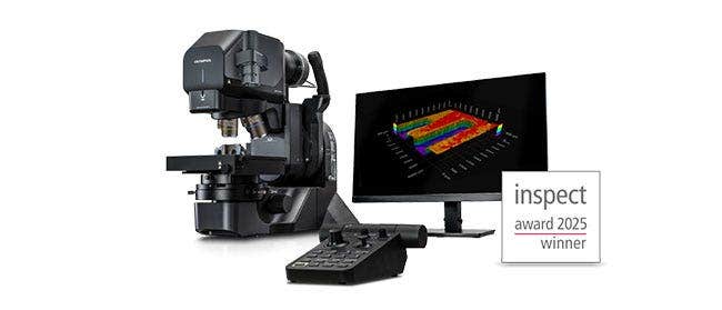
DSX2000
Digital Microscope Series
Our award-winning DSX2000 digital microscope series captures exceptional images that go beyond 4K digital imaging—simplifying industrial inspection tasks, boosting productivity and profitability, and streamlining workflows for QA/QC professionals. The DSX2000 fully motorized digital microscope integrates smart AI-powered tools, all-in-one digital imaging, and customizable interfaces into an industrial inspection solution ideal for electronics, automotive parts, metallurgical, and semiconductor inspection.
Designed for quick, accurate 2D and 3D digital measurement, the DSX2000 delivers exceptional high-resolution imaging, with a wide magnification range suited for accurate industrial inspection, quality control, failure analysis, and surface metrology. With 4K digital microscope cameras and a wide depth of field, the DSX2000 provides crystal-clear imaging of even the most complex materials and components.