Advanced Packaging Inspection and Metrology
Advanced packaging continues to push micro-bump pitches toward 20 µm and increase die stack height. The features that determine whether a package ships are now smaller than the ones most inspection benches were built for, and an increasing number sit under silicon, where a light microscope cannot follow.
Cross-sectioning can reveal these internal features, but only for the unit that was sectioned. Nondestructive inspection enables evaluation of these hidden features while keeping the parts intact. Selecting the appropriate inspection system depends on the feature of interest, its location, and its depth within the package.
Evident offers a wide range of advanced packaging inspection and metrology systems for precise imaging and 3D measurement of wire bonds, flip chips, redistribution layers (RDLs), and through-silicon vias (TSVs).
- Nondestructive: Use near-infrared imaging to inspect features through silicon while keeping the package intact.
- Quantitative: Measure 3D height, coplanarity, and step height without contacting the sample.
- Preemptive: Measure before reflow, molding, or subsequent layer bonding, when process adjustments can help reduce scrap and rework.
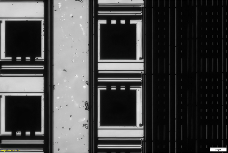
Near-infrared imaging reveals semiconductor features beneath silicon without sectioning the device.
What Each Packaging Technology Demands from Inspection
Advanced packaging requires inspection methods that can resolve fine surface details, reveal selected structures beneath silicon, and measure 3D surface geometry.
Inspection by Packaging Technology
Wire Bonding Inspection
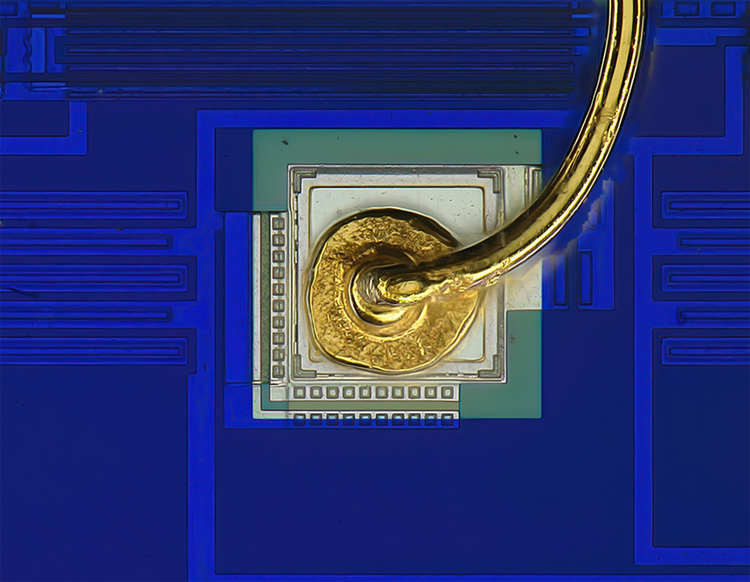
Ball bond and pad centering, imaged with the DSX2000 digital microscope.
The Challenge
Ball bonds must meet tight size, shape, and pad-centering tolerances. Incorrect loop height or wire sweep can cause wires to short against the die edge or become damaged during encapsulation.
How We Solve It
Wire bond quality is evaluated directly on the bonded device by measuring ball diameter, pad centering, loop height, and wire sweep. The STM7 measuring microscope supports precise three-axis measurements. The DSX2000 digital microscope adds 2D and 3D measurement, with depth of focus that keeps the full wire loop in view and a 21X to 7,300X range covering macro-to-micro inspection on one system.
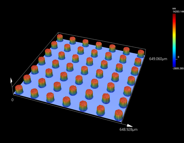
3D image of solder bumps on an integrated circuit, captured with the LEXT OLS5500 3D optical profilometer.
The Challenge
Bonding the flip chip dies face down hides the solder bumps beneath the silicon. Bump height and coplanarity must be checked before bonding, while post-bond inspection requires a nondestructive view of selected buried features.
How We Solve It
Before bonding, the LEXT™ OLS5500 3D optical profilometer measures bump height and coplanarity without contacting the sample. Setting a height reference plane measures every bump in the field of view at once, so a full field of 20 µm bumps is acquired in about 10 seconds.1 After bonding, the MX63 wafer inspection microscope configured for infrared observation uses near-infrared imaging through silicon up to 1.2 mm thick to observe selected buried features without sectioning.
1Based on Evident’s internal measurement.
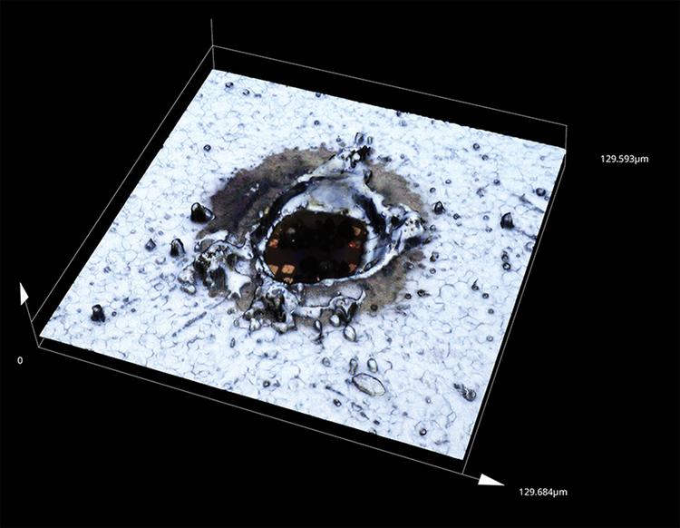
Laser mark on a bare semiconductor wafer imaged in 3D with the LEXT OLS5500 3D optical profilometer.
The Challenge
RDL patterning, bumping, and metallization occur while the dies remain in wafer form. Surface defects or height variations found late can put an entire wafer lot at risk.
How We Solve It
The DSX2000 digital microscope detects surface defects and contamination on bare wafers before processing starts. Particle detection in PRECiV™ software runs on a stitched image against a set threshold, and clicking a detected particle drives the stage to that location for confirmation. The LEXT™ OLS5500 3D optical profilometer provides noncontact measurement of RDL step height and bump profiles after patterning.
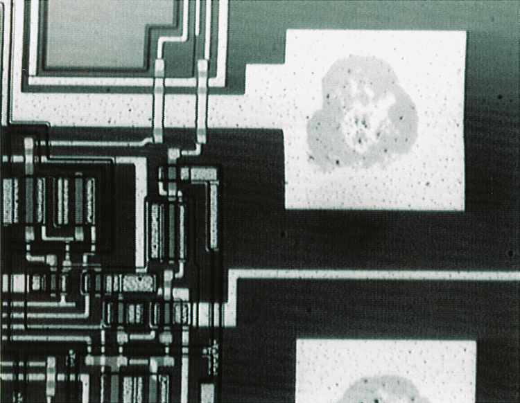
Circuit structures and bond pads seen through silicon, imaged with the BX53M upright microscope using IR objectives.
The Challenge
Fan-out wafer-level packaging places dies face-down on a carrier before molding them into a reconstituted wafer. Heating and cooling during molding warp the panel and shift the dies out of position, which throws off the alignment of the redistribution layer patterned on top.
How We Solve It
Near-infrared imaging locates each die through the carrier and silicon before RDL patterning, so a position error can be identified while correction is still possible. The MX63 microscope configured for infrared observation and the BX53M upright microscope with IR objectives support through-silicon inspection of alignment and circuit patterns, with IR objectives specified for silicon up to 1.2 mm thick.
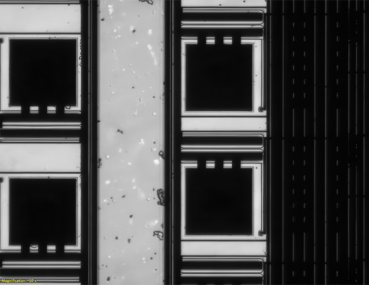
Circuit patterns and bond pads seen through silicon, imaged with the MX63 wafer inspection microscope using transmission infrared observation.
The Challenge
Multiple chiplets sit side by side on a silicon interposer and connect through TSVs and high-density RDL. A single broken trace or misaligned micro-bump can disrupt electrical connections and compromise a high-value completed module.
How We Solve It
Interposer traces and micro-bump alignment in 2.5D packages can be inspected at different stages of assembly. The MX63 microscope configured for infrared inspection scans the interposer RDL to identify shorts and opens. After chip-on-wafer bonding, its IR imaging mode enables inspection through the die to verify micro-bump alignment at approximately 20 to 40 µm pitch.
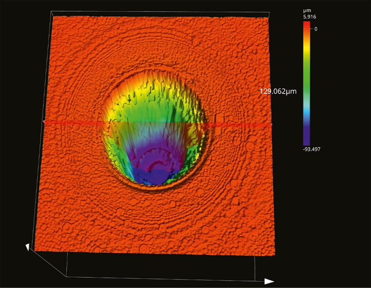
Three-dimensional image of a through-silicon via structure captured with the LEXT OLS5500 3D optical profilometer.
The Challenge
Stacked dies rely on through-silicon vias (TSVs) to connect multiple layers. Via depth and profile are verified after etch. After backside thinning, surface planarity and TSV protrusion must be evaluated, while buried fill defects require another inspection method.
How We Solve It
The LEXT OLS5500 3D optical profilometer provides noncontact measurement of TSV depth and profile, and of exposed TSV topography. The MX63 microscope uses differential interference contrast (DIC) to improve the visibility of minute surface-height differences. Subsurface TSV fill voids require acoustic or X-ray inspection.
Choosing the Right System for Your Packaging Process
The right inspection system depends on whether the target is visible on the surface, located beneath silicon, or defined by three-dimensional geometry.
1 Laser scanning microscopy 2 White light interferometry 3 Focus variation microscopy 4 The guaranteed accuracy and repeatability apply only if the device has been calibrated according to the manufacturer‘s specifications and is in defect-free condition. Calibration must be performed by an Evident technician or an Evident-authorized specialist.
Not Sure Which System Fits Your Process?
Tell us what you need to inspect, and we’ll help identify a suitable microscope configuration.
FAQs About Advanced Packaging Inspection and Metrology
Let’s Talk About Your Process
Every packaging line uses a different mix of technologies, tolerances, and throughput targets. Tell us what you need to inspect, and we’ll help identify a suitable microscope configuration.
Resources
Related Products
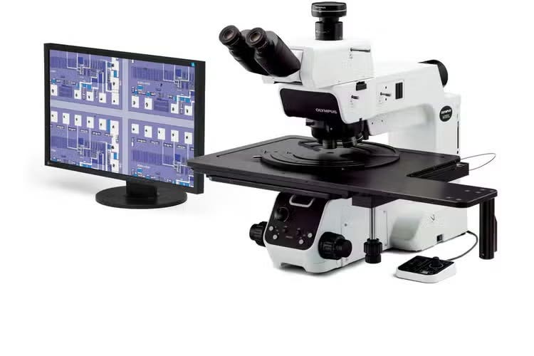
MX63-MX63L Wafer Inspection Microscope
STM7 microscopes offer excellent versatility and high-performance, three-axis measurements of parts and electrical components, with sub-micron precisi...
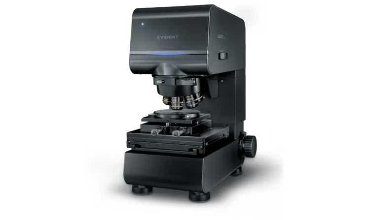
LEXT OLS5500 3D Optical Profilometer
The award-winning LEXT™ OLS5500 hybrid 3D optical profilometer unites laser scanning microscopy (LSM), white light interferometry (WLI), and focus variati...
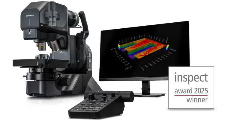
DSX2000 Digital Microscope
The DSX2000 fully motorized digital microscope series simplifies tasks, boosts productivity, and streamlines work for researchers and QC lab professio...
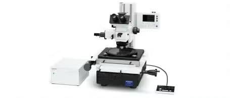
STM7 Measuring Microscope
STM7 microscopes offer excellent versatility and high-performance, three-axis measurements of parts and electrical components, with sub-micron precisi...
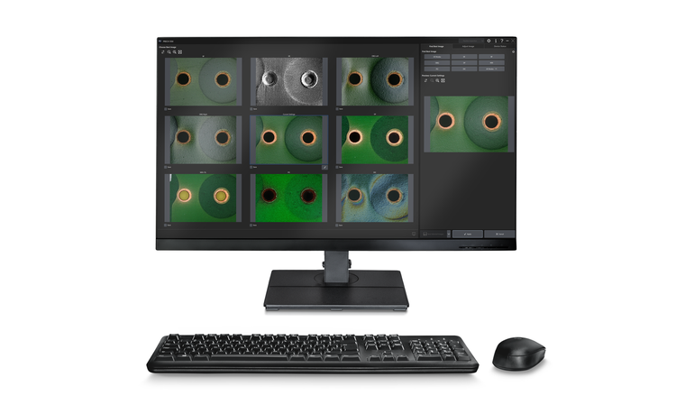
PRECiV Image Analysis Software
Evident image analysis software transforms microscopy images into actionable data for inspection, QC, and analysis tasks. Intuitive tools support...
Related Applications
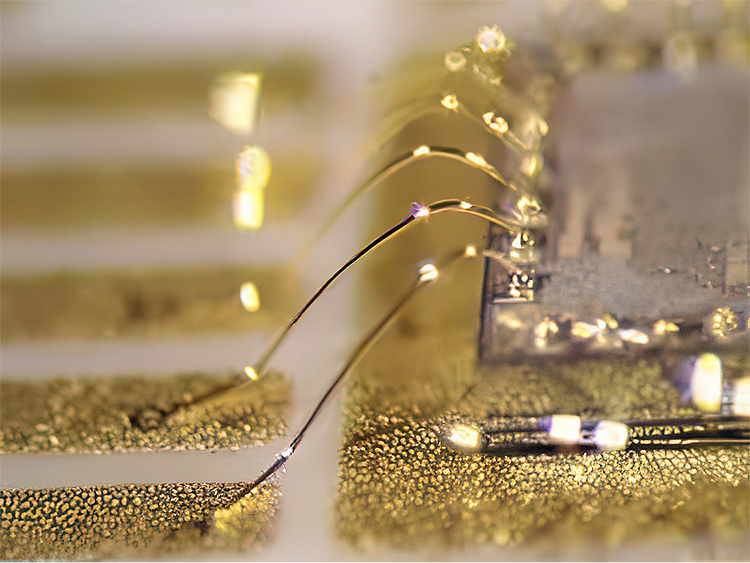
Inspecting Bonding Wires Using a Digital Microscope
Semiconductors are manufactured using a precise process. One step is wire bonding, where electrodes on an integrated circuit are connected to lead frames using soldered gold, aluminum, and copper wires. These wires can be as small as 10 µm in diameter and require a soldering accuracy as small as 2 to 3 µm. The level of precision necessary to solder the wires means that tiny vibrations can cause weak bonding, which, in turn, can cause the electronic device to fail.
Semiconductor Bare Wafer Lasermark
Marking wafers is an essential process in managing semiconductor wafer lots. Normally, silicon wafers are marked with their ID numbers using pulse laser irradiation. Laser irradiation creates dents in the lattice on a silicon wafer surface. These dents form a dot matrix sequence of characters and codes. In recent years, silicon wafers have continued to increase in density while at the same time becoming thinner. This has created a need to further reduce the size as well as to increase the accuracy of the laser marking technology.
BGA Cross Section Analysis
The packaging of electronic components on printed circuit boards (PCBs) has become denser due to the demand to make mobile electronic devices that are smaller and faster with increased functionality. Packaging methods for IC parts, in particular, have been shifting to bare chip packagig where IC chips are packaged directly on PCBs.